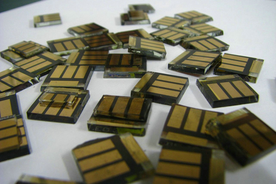
The perovskitiche cells are a particular type of photovoltaic cells that use as an absorbent material with a material structure perovskitca , or that has the same type of crystalline cell Catió 3 . On these cells, starting from 2009, intense research activity has been concentrated, thanks to the potential high efficiency, low production cost and ease of processing, characteristics that make it potentially very attractive from an industrial point of view.
In a few years they have achieved better results than organic cells and hybrid materials, achieving a maximum yield, reached in 2017, of 22.7%. Precisely these data make perovskite cells the solar technology that has marked the greatest development in recent years .
However, the transition to mass production has not yet been possible because the perovskitic solar cells present degradation problems, even losing 80% of the initial efficiency in the first 500 hours of use. Besides this, there are also other problems such as the presence of lead and the difficulty of forming very extensive layers.
History
The first use of perovskitic structure materials in photovoltaic cells dates back to 2009, when Miyasaka et al. incorporated in a Grätzel cell a perovskite hybrid based on organo-metal halides, using it as a dye on the mesoporous layer of TiO2 . With this cell, a yield (power conversion efficiency or PCE) of 3.8% was achieved. However, due to the redox solution present in the cell, the perovskitic coating remained stable for only a few minutes and eventually degraded.
After a period of stalemate in research, Park et al. in 2011 they improved this technology obtaining a 6.5% PCE but it remained the only article published on the subject in that year. Only a year later, Henry James Snaith and Mike Lee built a cell that replaced the redox solution present in the previous architecture, with a solid layer of a spiro-OMeTAD polymer that served as a conductor of holes (HTM) by reaching a PCE of 10% .
Subsequently, in 2013, both mesoporous and oxide-based technologies developed significantly, acting on different deposition methods and achieving efficiencies of 12-15%.
In December 2015 the efficiency record reached 21% up to 22.7% in 2017.
Characteristics of the most used perovskites
The real perovskite is a mineral found for the first time in 1839 on the Urals mountains, composed of a calcium oxide and titanium – CaTiO 3 which took its name from the Russian mineralogist Lev Perovski. This name has subsequently become synonymous with all those compounds that have the same crystallographic structure of the mineral: ABX 3where A is an atomic or molecular cation in the center of a cube, B are cations placed at the top of the cube and X smaller atoms negatively charged on the faces of the cube and which compose octahedral structures in B on each vertex of the cube. Depending on the type of atoms or molecules chosen, it is possible to obtain materials with peculiar and very interesting characteristics, such as superconductivity, photoluminescence, which allow their use in many fields.
In the case of perovskite solar cells the most salient and interesting results were obtained with hybrid organic-inorganic structures in which: A is an organic cation of methyl-ammonium, B is an inorganic cation generally Lead (+2), Tin or Germanium, while X is the halide anion (chloride, iodide, bromide).
The tolerance factor t is determinant in the structure of the perovskite and depends on the rays of the atomic / molecular species. The formula is given by:

Wherein r A , r B and r X are the radii of the respective ions. To obtain an ideal cubic structure, with maximum symmetry, the value of τ must be very close to 1; for this to be respected, ion A must be larger than ion B.
Since in the perovskites based on halides used in solar cells, site B is usually occupied by Pb or Sn which are already quite large atoms, an even larger molecule has been found to guarantee the stability of the cubic crystalline structure, such as methyl- ammonium. With a value of t between 0,89 and 1 there is a cubic structure while lower values lead to a less symmetric tetragonal or orthorombic structure. Typical t values of perovskites with halides are between 0.81 and 1.11. In these structures the octahedral factor m = r B / r X is between 0.44 and 0.90.
The most studied perovskitic compound that has allowed to obtain the best results is the tri-halide of Lead and methyl-ammonium , also referred to as MAPbX 3 ), characterized by an ideal band gap between 1.5 and 2.3 eV, able to provide high values of energy efficiency. The toxicity of Lead led to study perovskites based on other ions such as Tin (CH 3 NH 3 SnI 3 ) that have a potential band gap of 1.3 eV but which have lower efficiency values due to the variation of the electronic structure due to oxidation of the Tin ion from Sn +2 to Sn +4. At the same time, perovskites were studied in which the organic cation, methyl ammonium, was replaced with the larger formamidinium to increase its stability. Also compounds with co-presence of different anionic species such as bromide or iodide are being studied and have highlighted good characteristics and possibilities of applications.

Operating mechanism
As photovoltaic cells , even the operation of perovskite cells essentially leads to a direct conversion of solar radiation energy into electrical energy. Since there are currently developing perovskite cells with different architectures, and there is still debate about some aspects of the mechanism by which they work , we will focus on this section in delineating only the general aspects of its functioning.
In particular, in the figure we can see the current-voltage characteristic curve of a perovskitic cell based on , together with some figures of merit that well represent the typical values for this type of cells .

The generation of electric current from electromagnetic radiation within any type of photovoltaic cell can be schematically divided into three steps: photon absorption, separation of charges and transport of the latter. Below we will describe the characteristics of each of the three steps for the particular case of perovskite cells.
Absorption
In semiconductor and insulating materials , which therefore present a band gap at the Fermi level, an incoming photon with energy higher than that band gap can be absorbed, exciting an electronfrom the valence band (HOMO orbitals for discrete-level systems) to that , empty, conduction (LUMO orbitals for discrete level systems). These electrons, together with the electronic gaps left in the valence band, contribute to the electric current generated in the photovoltaic cells ( photovoltaic effect ).
A first important datum concerning the perovskites, and that differentiates them from the classic silicon modules, is the presence of a direct band gap (at least for the most used MAPbI3) which guarantees high absorption coefficients and therefore the possibility to have good performances absorption already with rather thin layers of material (typically a few hundred nm compared to hundreds of μm for conventional silicon) .
Now, given the solar spectrum, it is found that, for cells with a single absorbent material, an amplitude of band gap is ideal to maximize the power produced (in fact the quantity of absorbable frequencies, and therefore the current, is inversely proportional to the band gap amplitude, while the maximum voltage obtainable at the output of the cell is proportional to the bandgap amplitude). This ideal amplitude is calculated in approximately 1.4 eV, a value very close to the 1.55 eV of the most commonly used perovskites: . In particular, for the latter, the Shockley-Queisser limit is about 31% of efficiency for AM1.5 and 1000W / irradiated power conditions .

Regarding this aspect, another strength of perovskites, also interesting for tandem cells , is the possibility to vary band gap energy by varying the elements used in the structure or by using solid solutions of different perovskitic materials, as well as by varying parameters such as pressure and temperature .

Separation of charges
The excitation, by a photon, of an electron in the conduction band can generate, depending on the case: two independent charges (an electron in the conduction band and a gap in the valence band), or an exciton, or a linked electron-hole system. The first situation, typical of silicon, is the most efficient, as it produces almost free charges, and is the same that is found in the perovskite cells. In fact, the most commonly used perovskitic materials have in fact binding energies for very small electron-hole systems, of the order of at most 50 meV. These electron-hole systems are therefore approximable to almost free at room temperature (even if the bonding energy increases with decreasing dimensionality of the perovskitic absorber, this has not, however, prevented the development of cells with low-size perovskitic structures . ) .
Transport of charges
As a transport mechanism, a model has been proposed in which perovskite plays the role of an intrinsic layer in a pin junction , while the HTM and ETM layers (see cell architecture) respectively cover the role of semiconductors p and n (alternative models provide, for example, a ppn junction). Similarly to what happens in a conventional silicon cell, the charges are therefore definitively separated and attracted towards the respective electrodes by the built-in electric fields present in the junction, thus forming the photogenerated current .
This process is facilitated by the excellent properties of ambivalent conductors of the perovskites, which have high mean free walking values both for electrons and for holes (values in the literature indicate at least 100nm for , and above the μm for ), allowing therefore to use in the cells thickness of perovskites even of some hundreds of nanometers without significant recombination of the charge carriers, with consequent better absorption of solar radiation.


To further support the excellent conductive properties of the perovskites, DFT calculations have been performed which have shown, for the most used material, , rather low effective masses for both charge carriers ( and , where is it is the resting mass of the electron) .


On this basis we can therefore write the equations for the dynamics of electrons and gaps in stationary conditions inside the junction:


Where n (p) is the concentration of electrons (holes), D and μ are the diffusion and mobility coefficients, G and R the photogeneration and recombination coefficients considered dependent on the position. Finally, E is the electric field, which is also dependent on the position.
Typical approximations are to set R (x) = 0 (valid for thin absorber layers with respect to the average path of charges), ideal electric field (uniform) for pin junctions: , where is it is the potential difference built-in and the thickness of the area i. It can finally be placed according to the Lambert-Beer law . From these approximations we can arrive at analytical solutions for the current-voltage characteristics of the cells, solutions which, although they are rather complex, well reflect the real trend of these curves .


Cell architecture
The architectures of the cells based on an organic-inorganic semiconductor material, which has the polycrystalline structure of the perovskite (predominantly the ), can be mainly divided into two categories: those with a structure based on a mesoporous layer of a metal oxide (typically TiO 2 ) and those with planar heterojunctions .
Perovskitic cells based on a mesoporous metal oxide structure
In the first work of Miyasaka et al. the first use of the hybrid perovkitite is reported, in particular of the, as a dye in a Grätzel cell with liquid phase, reaching a conversion efficiency (PCE) of 3.81% with an almost complete coverage of the visible spectrum. Typically, this architecture consists of a sandwich structure, with a liquid electrolyte (mainly the redox pair I – / I 3 – ) between a counter electrode in Pt and an anode formed by a mesoporous layer of TiO 2 sensitized with the dye that has the role of solar radiation absorber.
A little while later, Park et al. manufactured the same type of cell, with the difference that they used quantum dots (QDs) perovskitici of 2-3 nm on a mesoporous layer of about 3.6 μm of TiO 2 , succeeding in bringing the PCE to 6.54% but highlighting the problem of this type of architecture: the presence of the electrolyte gradually dissolved the perovskite leading to a rapid reduction in efficiency.
For this reason, Grätzel and Park et al. completely changed the cell architecture, moving to the solid-state Grätzel cell architecture. In this configuration, inside the pore of TiO 2 and above the mesoporous layer and a perovskitic layer, a material was added to capture and transport the generated holes (hole transport material, HTM), a polymer called spiro-MeOTAD, which brought the PCE to reach values close to 9.7%. Higher PCE values were then obtained, again in the same configuration, replacing the Spiro-Meotad with other organic compounds such as PTAA (poly-triarylamine) or pyrene derivatives , reaching a PCE of 15%.
These architectures, illustrated up to now, are part of the so-called solar cells with an “active” mesoporous layer, in the sense that the mesoporous oxide layer actively participates in the separation of the electron- moon pair .
Also in the same period, Lee et al. used Al 2 O 3 instead of TiO 2 with a mixed hybrid perovskite always coupled with a layer of spiro-MeOTAD reaching 10.9% PCE and obtaining what have been called meso-structured solar cells (MSSCs). These are always classified as solar cells with a mesoporous layer, but this time the layer is called “passive” in the sense that it serves only as a support for the perovskite, which in this case does not only serve as dye but also as conveyor of the generated charges. This discovery has in a very short time led to the awareness of being able to obtain cells that did not have a mesoporous structure but, on the contrary, consisted of a perovskite film, obtaining planar heterojunction cells (planar heterojunction solar cells PHJ ).
Perovskitic cells based on planar eterojunctions
The first attempt was carried out always by the work of Lee et al which however obtained a very low PCE of 1.8% due to the difficult homogenization of the deposited layer; only later, they always managed to reach values of 11.4% only by optimizing the formation of the layer. PHJ solar cells are divided into two categories according to the layers’ packing and are the nip structure and the “inverted” pin structure.
Nip structure
Normally, the architecture of this type of cell is composed of a continuous layer of perovskite that is directly in contact with a compact layer of TiO 2and a layer of HTM. In conventional structures (nip), in most cases the structure of cells with active mesoporous layer is inherited: essentially, a n-type layer used for the electron transport function (electron transporting materials ETM) is deposited on a transparent substrate. and conductive that acts as an electrode. The perovskite layer, the layer for transporting the holes (HTM) and finally the counter-electrode are positioned above the type-n layer. The most used materials like ETM are titanium oxide (mainly used), zinc oxide, or II-VI nanoparticles (eg CdSe); while among the HTM we find the famous spiro-MeOTAD with other organic molecules such as P3HT or of the hydrophobic derivatives of oligothiophene (DR3TBDTT).
Pin structure
The pin structures are also called “inverted” because they have the order reversed compared to the nips and were first developed by Guo et al in 2013. The first pin used a perovskite between a polymer with a p-type doping . (PEDOT: PSS) and a derivative of fullerene with n-type doping (PC 61 BM) only that in this case the light first passes through the p-doped layer as opposed to what happened previously. 5Although the PCE of this first cell was smaller than the mesoporous ones, this work was of considerable importance because it was the first cell to be built at a T <150 ° C. Starting from this then, many different architectures developed that brought the PCE to much higher levels and at present, this type of cells are the most promising.
Since perovskite can itself act as HTM, architecture has also been developed without any HTM from Etgar at, which achieved an 8% PCE.
Deposition processes
There are several methods for making perovskites . Among these, those mainly used are:
– spin coating from one- or two-step chemical solutions
– sequential process
– double source vapor phase deposition
– assisted deposition by vapor phase
In the following treatment of the methods the formation of the perovskitic film MAPbI 3 (ie)
Spin coating : as regards the one-step method, the precursors of pervoskite (PbI and MAI) are dissolved in a common solvent which in most cases is dimethylformamide (DMF) or Butyloractone. Then the solution obtained is deposited on the substrates by spinning. The rotation of the sample is very rapid and this allows to spread the fluid on the subrato thanks to the centrifugal force. During the process the film can be thinned due to the evaporation of solvents, which are often very volatile. To guarantee the formation of a substantial film a percentage of mass in solution of about 40% is required.
Once the film has been deposited, it is placed inside a heater (annealing phase) which completes the formation of the perovskite.
The two-step spin coating process instead involves the deposition, at different times, of the two solutions (for example PbI / DMF and MAI / isopropyl alcohol (IPA))
Seialial process : initially we proceed by depositing the PbI / DMF solution (the first precursor) by means of spinning; Subsequently the substrate is immersed (dipping) in a second solution containing MAI and isopropyl alcohol (MAI / IPA, the second precursor). And this is where the on site reaction occurs with the formation of the perovskite. The process is concluded by using a heater which, unlike the previous method, has the sole purpose of eliminating any traces of residual solvent.
This method allows a better control of the morphology with respect to spin coating, thus avoiding the occurrence of greater unevenness in the thickness of the perovskite which would lead to a worse functioning of the cell.
Dual source vapor deposition : it is currently the most expensive method but promises notable future developments. The process involves inserting our substrate into a machine (kept under high vacuum conditions) which will form the vapors of the two precursors of our interest (for example PbI 2 and MAI) and then shoot them against the substrate. in such a way as to make them interact, react and finally deposit. Compared to the previous methods, this is the best in terms of uniformity of film coverage on the substrate.
Assisted vapor phase deposition: this method combines the sequential process and the vapor phase assisted deposition. The lead halide is deposited by spin coating and then the MAI is vaporized on the PbI at 150 ° C for at least 2 hours in a nitrogen atmosphere in order to convert it all into perovskite.
Exactly as for the double-source vapor deposition (and in general for all the vapor phase deposition processes), the film’s supercial coverage is greater than that found in the films processed by means of solutions.
Problems
The simplicity of the manufacturing technique and the combination of relevant properties, such as the direct band-gap, the high absorption coefficients, the ambipolar charge transport property, the high values of the open circuit voltage and the charge mobility, have made the material with a highly competitive perovskitic structure compared to conventional semiconductors. Despite this, there are still many factors to be optimized to allow a concrete industrialization: long-term stability, the choice of an alternative material to lead, the excessive cost for completing the cell, such as the choice of the layer transporters of holes (hole transport material, HTM, generally organic materials) and electrical contact for the collection of charges (precious metals such as gold, silver).
A major challenge for perovskite solar cells (PSCs) is the aspect of short- and long-term stability. The instability of the PSCs is mainly related to the environmental influence (humidity and oxygen), thermal influence (intrinsic stability), heating under applied voltage, photographic influence (ultraviolet light) and fragility mechanics.
An important factor in the operation of any device is that it is stable in air without the use of any type of encapsulation. Yang et al compared the devices stored in dry air and in a nitrogen atmosphere and showed that air degradation of the Omos (organometal halide) peroskitic material occurred, thus highlighting the need for protection . Recently, it has been shown that encapsulation of the perovskite absorber with a carbon nanotube composite and an inert polymer matrix successfully prevents the immediate degradation of the material exposed to moist air at elevated temperatures. Carbon nanotubes, in fact, make the cell more stable even in conditions of full solar irradiation. However, long-term studies and complete encapsulation techniques for perovskite solar cells have not yet been demonstrated.
In the case of moisture, it has been discovered that it has both positive and negative effects on perovskite solar cells. The manufacturing process in film formation and grain edge movement under controlled humidity conditions lead to large crystal formation and reduced film pinholes. This film reconstruction accelerates the nucleation and crystallization of the perovskite phase. A small amount of water helps make smooth and dense perovskite films.
However, humidity remains one of the main reasons for the degradation of the Omh-PSC. Seok et al. recommend the manufacture of Omh-PSC in a controlled atmosphere with a moisture level of less than 1%.
UV illumination can reduce PSC performance as a result of exposure during long-term operation. In the realization of devices in which the mesoporous layer of TiO2 is sensitized with a perovskite absorber, UV instability is noted. The cause of the observed decline in the performance of the device of such solar cells is related to the interaction between the photogenerated holes inside the TiO2 and the oxygen radicals on the surface of the TiO2. The extremely low thermal conductivity measured of 0.5 W / (km) at room temperature in CH3NH3PbI3, can prevent rapid propagation of heat deposited by light and keep the cell resistive to thermal stresses that can reduce its duration. The PbI2 residue in perovskite film has experimentally demonstrated to have a negative effect on the long-term stability of the devices. It is believed that the stabilization problem is solved by replacing the organic transport layer with a metal oxide layer, allowing the cell to retain 90% capacity after 60 days.
The field of PSCs is undergoing rapid development and most research efforts are focused on making devices with better efficiencies. An equally vital topic on which we focus is the improvement of stability. Good results have already been achieved, as we have moved from a few minutes to thousands of hours (2000 h). The knowledge of degradation mechanisms, structures and phase transformations under different operating conditions play a key role in the prediction of the material and in the behavior of the device.
Source from Wikipedia