The theory of solar cells explains the process by which light energy in photons is converted into electric current when the photons strike a suitable semiconductor device. The theoretical studies are of practical use because they predict the fundamental limits of a solar cell, and give guidance on the phenomena that contribute to losses and solar cell efficiency.
Simple explanation
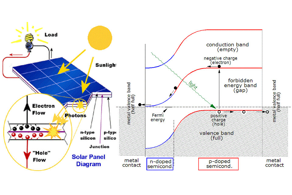
Photons in sunlight hit the solar panel and are absorbed by semi-conducting materials.
Electrons (negatively charged) are knocked loose from their atoms as they are excited. Due to their special structure and the materials in solar cells, the electrons are only allowed to move in a single direction. The electronic structure of the materials is very important for the process to work, and often silicon incorporating small amounts of boron or phosphorus is used in different layers.
An array of solar cells converts solar energy into a usable amount of direct current (DC) electricity.
Photogeneration of charge carriers
When a photon hits a piece of silicon, one of three things can happen:
The photon can pass straight through the silicon — this (generally) happens for lower energy photons.
The photon can reflect off the surface.
The photon can be absorbed by the silicon if the photon energy is higher than the silicon band gap value. This generates an electron-hole pair and sometimes heat depending on the band structure.
When a photon is absorbed, its energy is given to an electron in the crystal lattice. Usually this electron is in the valence band. The energy given to the electron by the photon “excites” it into the conduction band where it is free to move around within the semiconductor. The network of covalent bonds that the electron was previously a part of now has one fewer electron. This is known as a hole. The presence of a missing covalent bond allows the bonded electrons of neighboring atoms to move into the “hole,” leaving another hole behind, thus propagating holes throughout the lattice. It can be said that photons absorbed in the semiconductor create electron-hole pairs.
A photon only needs to have energy greater than that of the band gap in order to excite an electron from the valence band into the conduction band. However, the solar frequency spectrum approximates a black body spectrum at about 5,800 K, and as such, much of the solar radiation reaching the Earth is composed of photons with energies greater than the band gap of silicon. These higher energy photons will be absorbed by the solar cell, but the difference in energy between these photons and the silicon band gap is converted into heat (via lattice vibrations — called phonons) rather than into usable electrical energy. The photovoltaic effect can also occur when two photons are absorbed simultaneously in a process called two-photon photovoltaic effect. However, high optical intensities are required for this nonlinear process.
The p-n junction
The most commonly known solar cell is configured as a large-area p-n junction made from silicon. As a simplification, one can imagine bringing a layer of n-type silicon into direct contact with a layer of p-type silicon. In practice, p-n junctions of silicon solar cells are not made in this way, but rather by diffusing an n-type dopant into one side of a p-type wafer (or vice versa).
If a piece of p-type silicon is placed in close contact with a piece of n-type silicon, then a diffusion of electrons occurs from the region of high electron concentration (the n-type side of the junction) into the region of low electron concentration (p-type side of the junction). When the electrons diffuse across the p-n junction, they recombine with holes on the p-type side. However (in the absence of an external circuit) this diffusion of carriers does not go on indefinitely because charges build up on either side of the junction and create an electric field. The electric field promotes charge flow, known as drift current, that opposes and eventually balances out the diffusion of electrons and holes. This region where electrons and holes have diffused across the junction is called the depletion region because it contains practically no mobile charge carriers. It is also known as the space charge region, although space charge extends a bit further in both directions than the depletion region.
Charge carrier separation
There are two causes of charge carrier motion and separation in a solar cell:
drift of carriers, driven by the electric field, with electrons being pushed one way and holes the other way
diffusion of carriers from zones of higher carrier concentration to zones of lower carrier concentration (following a gradient of electrochemical potential).
These two “forces” may work one against the other at any given point in the cell. For instance, an electron moving through the junction from the p region to the n region (as in the diagram at the beginning of this article) is being pushed by the electric field against the concentration gradient. The same goes for a hole moving in the opposite direction.
It is easiest to understand how a current is generated when considering electron-hole pairs that are created in the depletion zone, which is where there is a strong electric field. The electron is pushed by this field toward the n side and the hole toward the p side. (This is opposite to the direction of current in a forward-biased diode, such as a light-emitting diode in operation.) When the pair is created outside the space charge zone, where the electric field is smaller, diffusion also acts to move the carriers, but the junction still plays a role by sweeping any electrons that reach it from the p side to the n side, and by sweeping any holes that reach it from the n side to the p side, thereby creating a concentration gradient outside the space charge zone.
In thick solar cells there is very little electric field in the active region outside the space charge zone, so the dominant mode of charge carrier separation is diffusion. In these cells the diffusion length of minority carriers (the length that photo-generated carriers can travel before they recombine) must be large compared to the cell thickness. In thin film cells (such as amorphous silicon), the diffusion length of minority carriers is usually very short due to the existence of defects, and the dominant charge separation is therefore drift, driven by the electrostatic field of the junction, which extends to the whole thickness of the cell.
Once the minority carrier enters the drift region, it is ‘swept’ across the junction and, at the other side of the junction, becomes a majority carrier. This reverse current is a generation current, fed both thermally and (if present) by the absorption of light. On the other hand, majority carriers are driven into the drift region by diffusion (resulting from the concentration gradient), which leads to the forward current; only the majority carriers with the highest energies (in the so-called Boltzmann tail; cf. Maxwell–Boltzmann statistics) can fully cross the drift region. Therefore, the carrier distribution in the whole device is governed by a dynamic equilibrium between reverse current and forward current.
Connection to an external load
Ohmic metal-semiconductor contacts are made to both the n-type and p-type sides of the solar cell, and the electrodes connected to an external load. Electrons that are created on the n-type side, or created on the p-type side, “collected” by the junction and swept onto the n-type side, may travel through the wire, power the load, and continue through the wire until they reach the p-type semiconductor-metal contact. Here, they recombine with a hole that was either created as an electron-hole pair on the p-type side of the solar cell, or a hole that was swept across the junction from the n-type side after being created there.
The voltage measured is equal to the difference in the quasi Fermi levels of the majority carriers (electrons in the n-type portion and holes in the p-type portion) at the two terminals.
Equivalent circuit of a solar cell
To understand the electronic behavior of a solar cell, it is useful to create a model which is electrically equivalent, and is based on discrete ideal electrical components whose behavior is well defined. An ideal solar cell may be modelled by a current source in parallel with a diode; in practice no solar cell is ideal, so a shunt resistance and a series resistance component are added to the model. The resulting equivalent circuit of a solar cell is shown on the left. Also shown, on the right, is the schematic representation of a solar cell for use in circuit diagrams.
Characteristic equation
From the equivalent circuit it is evident that the current produced by the solar cell is equal to that produced by the current source, minus that which flows through the diode, minus that which flows through the shunt resistor:
where

I = output current (ampere)
IL = photogenerated current (ampere)
ID = diode current (ampere)
ISH = shunt current (ampere).
The current through these elements is governed by the voltage across them:
where

Vj = voltage across both diode and resistor RSH (volt)
V = voltage across the output terminals (volt)
I = output current (ampere)
RS = series resistance (Ω).
By the Shockley diode equation, the current diverted through the diode is:
where
![{\displaystyle I_{D}=I_{0}\left\{\exp \left[{\frac {V_{j}}{nV_{T}}}\right]-1\right\}}](https://wikimedia.org/api/rest_v1/media/math/render/svg/0b50e360bdf5d4b6a17729bcfddff18aba2151d9)
I0 = reverse saturation current (ampere)
n = diode ideality factor (1 for an ideal diode)
q = elementary charge
k = Boltzmann’s constant
T = absolute temperature
the thermal voltage. At 25 °C, volt.
By Ohm’s law, the current diverted through the shunt resistor is:
 the thermal voltage. At 25 °C,
where

RSH = shunt resistance (Ω).
Substituting these into the first equation produces the characteristic equation of a solar cell, which relates solar cell parameters to the output current and voltage:
An alternative derivation produces an equation similar in appearance, but with V on the left-hand side. The two alternatives are identities; that is, they yield precisely the same results.
![{\displaystyle I=I_{L}-I_{0}\left\{\exp \left[{\frac {V+IR_{S}}{nV_{T}}}\right]-1\right\}-{\frac {V+IR_{S}}{R_{SH}}}.}](https://wikimedia.org/api/rest_v1/media/math/render/svg/703f9ec7a22125aac0ba9e627bb9dbfcc069c495)
Since the parameters I0, n, RS, and RSH cannot be measured directly, the most common application of the characteristic equation is nonlinear regression to extract the values of these parameters on the basis of their combined effect on solar cell behavior.
When RS is not zero, the above equation does not give the current I directly, but it can then be solved using the Lambert W function:
When an external load is used with the cell, its resistance can simply be added to RS and V set to zero in order to find the current.

When RSH is infinite there is a solution for V for any less than :

 :
:
Otherwise one can solve for V using the Lambert W function:

However, when RSH is large it’s better to solve the original equation numerically.

The general form of the solution is a curve with I decreasing as V increases. The slope at small or negative V (where the W function is near zero) approaches , whereas the slope at high V approaches .


Open-circuit voltage and short-circuit current
When the cell is operated at open circuit, I = 0 and the voltage across the output terminals is defined as the open-circuit voltage. Assuming the shunt resistance is high enough to neglect the final term of the characteristic equation, the open-circuit voltage VOC is:
Similarly, when the cell is operated at short circuit, V = 0 and the current I through the terminals is defined as the short-circuit current. It can be shown that for a high-quality solar cell (low RS and I0, and high RSH) the short-circuit current ISC is:

It is not possible to extract any power from the device when operating at either open circuit or short circuit conditions.

Effect of physical size
The values of IL, I0, RS, and RSH are dependent upon the physical size of the solar cell. In comparing otherwise identical cells, a cell with twice the junction area of another will, in principle, have double the IL and I0 because it has twice the area where photocurrent is generated and across which diode current can flow. By the same argument, it will also have half the RS of the series resistance related to vertical current flow; however, for large-area silicon solar cells, the scaling of the series resistance encountered by lateral current flow is not easily predictable since it will depend crucially on the grid design (it is not clear what “otherwise identical” means in this respect). Depending on the shunt type, the larger cell may also have half the RSH because it has twice the area where shunts may occur; on the other hand, if shunts occur mainly at the perimeter, then RSH will decrease according to the change in circumference, not area.
Since the changes in the currents are the dominating ones and are balancing each other, the open-circuit voltage is practically the same; VOC starts to depend on the cell size only if RSH becomes too low. To account for the dominance of the currents, the characteristic equation is frequently written in terms of current density, or current produced per unit cell area:
where
J = current density (ampere/cm2)
JL = photogenerated current density (ampere/cm2)
J0 = reverse saturation current density (ampere/cm2)
rS = specific series resistance (Ω-cm2)
rSH = specific shunt resistance (Ω-cm2).
![J=J_{{L}}-J_{{0}}\left\{\exp \left[{\frac {q(V+Jr_{{S}})}{nkT}}\right]-1\right\}-{\frac {V+Jr_{{S}}}{r_{{SH}}}}](https://wikimedia.org/api/rest_v1/media/math/render/svg/b907809fa1123fb91843d5612e8b45df5d7e8e21)
This formulation has several advantages. One is that since cell characteristics are referenced to a common cross-sectional area they may be compared for cells of different physical dimensions. While this is of limited benefit in a manufacturing setting, where all cells tend to be the same size, it is useful in research and in comparing cells between manufacturers. Another advantage is that the density equation naturally scales the parameter values to similar orders of magnitude, which can make numerical extraction of them simpler and more accurate even with naive solution methods.
There are practical limitations of this formulation. For instance, certain parasitic effects grow in importance as cell sizes shrink and can affect the extracted parameter values. Recombination and contamination of the junction tend to be greatest at the perimeter of the cell, so very small cells may exhibit higher values of J0 or lower values of RSH than larger cells that are otherwise identical. In such cases, comparisons between cells must be made cautiously and with these effects in mind.
This approach should only be used for comparing solar cells with comparable layout. For instance, a comparison between primarily quadratical solar cells like typical crystalline silicon solar cells and narrow but long solar cells like typical thin film solar cells can lead to wrong assumptions caused by the different kinds of current paths and therefore the influence of, for instance, a distributed series resistance contribution to rS. Macro-architecture of the solar cells could result in different surface areas being placed in any fixed volume – particularly for thin film solar cells and flexible solar cells which may allow for highly convoluted folded structures. If volume is the binding constraint, then efficiency density based on surface area may be of less relevance.
Transparent conducting electrodes
Transparent conducting electrodes are essential components of solar cells. It is either a continuous film of indium tin oxide or a conducting wire network, in which wires are charge collectors while voids between wires are transparent for light. An optimum density of wire network is essential for the maximum solar cell performance as higher wire density blocks the light transmittance while lower wire density leads to high recombination losses due to more distance traveled by the charge carriers.
Cell temperature
Temperature affects the characteristic equation in two ways: directly, via T in the exponential term, and indirectly via its effect on I0 (strictly speaking, temperature affects all of the terms, but these two far more significantly than the others). While increasing T reduces the magnitude of the exponent in the characteristic equation, the value of I0 increases exponentially with T. The net effect is to reduce VOC (the open-circuit voltage) linearly with increasing temperature. The magnitude of this reduction is inversely proportional to VOC; that is, cells with higher values of VOC suffer smaller reductions in voltage with increasing temperature. For most crystalline silicon solar cells the change in VOC with temperature is about -0.50%/°C, though the rate for the highest-efficiency crystalline silicon cells is around -0.35%/°C. By way of comparison, the rate for amorphous silicon solar cells is -0.20%/°C to -0.30%/°C, depending on how the cell is made.
The amount of photogenerated current IL increases slightly with increasing temperature because of an increase in the number of thermally generated carriers in the cell. This effect is slight, however: about 0.065%/°C for crystalline silicon cells and 0.09% for amorphous silicon cells.
The overall effect of temperature on cell efficiency can be computed using these factors in combination with the characteristic equation. However, since the change in voltage is much stronger than the change in current, the overall effect on efficiency tends to be similar to that on voltage. Most crystalline silicon solar cells decline in efficiency by 0.50%/°C and most amorphous cells decline by 0.15-0.25%/°C. The figure above shows I-V curves that might typically be seen for a crystalline silicon solar cell at various temperatures.
Series resistance
As series resistance increases, the voltage drop between the junction voltage and the terminal voltage becomes greater for the same current. The result is that the current-controlled portion of the I-V curve begins to sag toward the origin, producing a significant decrease in the terminal voltage and a slight reduction in ISC, the short-circuit current. Very high values of RS will also produce a significant reduction in ISC; in these regimes, series resistance dominates and the behavior of the solar cell resembles that of a resistor. These effects are shown for crystalline silicon solar cells in the I-V curves displayed in the figure to the right.
 and a slight reduction in ISC, the short-circuit current. Very high values of RS will also produce a significant reduction in ISC; in these regimes, series resistance dominates and the behavior of the solar cell resembles that of a resistor. These effects are shown for crystalline silicon solar cells in the I-V curves displayed in the figure to the right.
Losses caused by series resistance are in a first approximation given by Ploss=VRsI=I2RS and increase quadratically with (photo-)current. Series resistance losses are therefore most important at high illumination intensities.
Shunt resistance
As shunt resistance decreases, the current diverted through the shunt resistor increases for a given level of junction voltage. The result is that the voltage-controlled portion of the I-V curve begins to sag far from the origin, producing a significant decrease in the terminal current I and a slight reduction in VOC. Very low values of RSH will produce a significant reduction in VOC. Much as in the case of a high series resistance, a badly shunted solar cell will take on operating characteristics similar to those of a resistor. These effects are shown for crystalline silicon solar cells in the I-V curves displayed in the figure to the right.
Reverse saturation current
If one assumes infinite shunt resistance, the characteristic equation can be solved for VOC:
Thus, an increase in I0 produces a reduction in VOC proportional to the inverse of the logarithm of the increase. This explains mathematically the reason for the reduction in VOC that accompanies increases in temperature described above. The effect of reverse saturation current on the I-V curve of a crystalline silicon solar cell are shown in the figure to the right. Physically, reverse saturation current is a measure of the “leakage” of carriers across the p-n junction in reverse bias. This leakage is a result of carrier recombination in the neutral regions on either side of the junction.

Ideality factor
The ideality factor (also called the emissivity factor) is a fitting parameter that describes how closely the diode’s behavior matches that predicted by theory, which assumes the p-n junction of the diode is an infinite plane and no recombination occurs within the space-charge region. A perfect match to theory is indicated when n = 1. When recombination in the space-charge region dominate other recombination, however, n = 2. The effect of changing ideality factor independently of all other parameters is shown for a crystalline silicon solar cell in the I-V curves displayed in the figure to the right.
Most solar cells, which are quite large compared to conventional diodes, well approximate an infinite plane and will usually exhibit near-ideal behavior under Standard Test Condition (n ≈ 1). Under certain operating conditions, however, device operation may be dominated by recombination in the space-charge region. This is characterized by a significant increase in I0 as well as an increase in ideality factor to n ≈ 2. The latter tends to increase solar cell output voltage while the former acts to erode it. The net effect, therefore, is a combination of the increase in voltage shown for increasing n in the figure to the right and the decrease in voltage shown for increasing I0 in the figure above. Typically, I0 is the more significant factor and the result is a reduction in voltage.
Sometimes, the ideality factor is observed to be greater than 2, which is generally attributed to the presence of Schottky diode or heterojunction in the solar cell. The presence of a heterojunction offset reduces the collection efficiency of the solar cell and may contribute to low fill-factor.
Source from Wikipedia